Intel said that it will introduce a 10-nanometer (nm) manufacturing process for its chips this year that will give it a 30 percent cost advantage, as well as a performance advantage over its rivals.
While Qualcomm announced earlier this year it was shipping a 10-nm processor in 2017 (based on a Samsung manufacturing process), Intel said that rivals aren’t using the same terminology as it does. Intel claimed that on every technical measure, from gate pitch to the number of transistors that can be put in a given area, it has an advantage.
Kaizad Mistry, corporate vice president in Intel’s logic technology group, echoed other executives in saying Intel’s 10-nm process, which will hit volume production this year, will be better than competitors’. He spoke at a press event in San Francisco.
Intel competes with rivals such as Global Foundries, TSMC, and Samsung in manufacturing chips. Intel’s product rivals, such as Qualcomm and Advanced Micro Devices, use those manufacturers to make their competing chips.
June 5th: The AI Audit in NYC
Join us next week in NYC to engage with top executive leaders, delving into strategies for auditing AI models to ensure fairness, optimal performance, and ethical compliance across diverse organizations. Secure your attendance for this exclusive invite-only event.
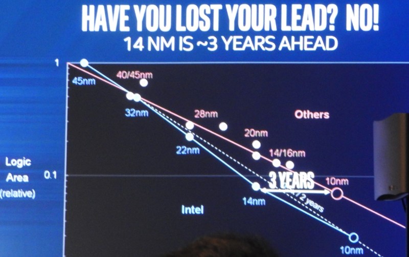
Above: Intel is on the blue path, and rivals are behind on the red path, in this Intel graph.
A nanometer is a billionth of a meter, and it only takes four silicon atoms in a crystal lattice to make one nanometer. In a 10-nm process, the circuits are only 10 nm apart. This should be easy to measure, and Intel called for a standard measurement for the industry, but the other companies in the industry are using a different description, Intel fellow Mark Bohr said during the event.
Intel said that it is still living up to the prediction of Moore’s Law, the prescient forecast made by Intel chairman emeritus Gordon Moore in 1965. Moore predicted the number of transistors on a chip would double every couple of years, and the industry has done that. By doubling the transistor count so regularly, the electronics industry has reaped huge benefits.
“People have been saying that Moore’s Law is dead for years, and the industry has always proved them wrong,” said Dan Hutcheson, chip analyst and CEO at VLSI Research in San Jose, Calif.
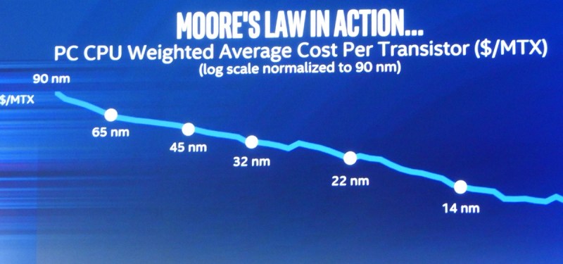
Above: Progress on Moore’s Law is intact, but not always steady.
By putting miniaturizing transistors, Intel can put more of them in the same space. Each transistor is smaller and closer to each other, which reduces the distance an electronic signal must travel. That makes the chip faster. It also reduces cost, as it takes less material to make a given number of transistors on a chip. So when Intel moves from one generation to another, like from 14-nm chips to 10-nm, the chips get smaller, cheaper, and faster.
Intel executive vice president Stacy Smith said that if every industry had moved forward on the same line as the chip industry has, we would be able to travel to the sun on a single gallon of gas, feed the world’s population on a square kilometer of land, and travel at 300 times the speed of light.
When Intel didn’t move to 10-nm chips earlier, a number of industry observers worried that Intel was falling off the pace of Moore’s Law and that electronics progress would slow down as a result.
But today, Intel executives said that, while it is taking longer for the company to get to 10-nm chips, those chips will have 2.7 times the transistor density of the previous generation, instead of the usual two times every couple of years. And so Intel says it remains on the predicted path in the long run. In other words, Moore’s Law isn’t foreordained. It is dependent on engineering advances that aren’t completely predictable from generation to generation, but have happened remarkably regularly over time.
“This is really, really important,” said Mistry. “The economic benefits of Moore’s Law are intact.”
Intel credits “hyper scaling” for extracting the full cost per transistor benefit of advanced patterning schemes. The Moore’s Law advances would not be possible without a combination of advances such as self-aligned double patterning.
This technique uses a spacer material to create features on a chip with half the original lithographic pitch, allowing better pitch scaling than another prevailing method (dubbed litho-etch-litho-etch, or LELE).
Intel is also using multiple dimensions to pack the electronics more efficiently. The 10-nm technology will use Intel’s third generation of FinFET (something Intel called tri-gate in the past) manufacturing. First introduced in 2011, FinFET is a transistor structure that takes advantage of three dimensions in a logic gate (which consists of transistors). This method improves performance and reduces power consumption over the traditional planar transistor used by the industry before 2011.
Intel has a gate pitch of 54 nm, which Intel says is the tightest metal pitch (distance between circuits) in the industry, Mistry said. Hutcheson at VLSI Research said he agreed that, based on Intel’s presentation, it appears to be a generation ahead of its rivals.
We asked Qualcomm for comment, and we have not had a response yet. But one Intel rival sent us a message.
“We are pleased to see competitors following our lead with the introduction of low-power 22nm processes. Almost two years ago, we launched our 22FDX FD-SOI technology for wireless, battery-powered intelligent systems,” said Alain Mutricy, senior vice president of product management group at Global Foundries. “We chose FD-SOI over bulk planar or FinFET because it provides the best combination of performance, power and area for these applications. Our process is fully qualified for production and we are seeing strong customer demand, with more than 50 active engagements in high-growth areas such as mobile, IoT, and automotive.”
Intel plans to use its manufacturing prowess to serve other chip design companies. It is operating as a foundry, where it makes chips designed and sold by other companies. Murthy Renduchintala, president of a number of Intel businesses, said that Intel is pursuing more customers for that business.
He also said that Intel’s chip designers also have to innovate with chip designs in order to take advantage of the manufacturing advantage.
“Our strategy isn’t based on one golden arrow,” Renduchintala said. “We have to count on multiple golden arrows.”