IBM Research and partners GlobalFoundries and Samsung have created transistors for a 5-nanometer semiconductor chip.
It’s a remarkable technical achievement, though a commercial version of the chip may not be possible for a while. Still, it should enable chips with 30 billion transistors, the on-off switches of electronic devices, on a fingernail-sized chip. Researchers say this kind of achievement should enable the $330 billion chip industry to stay on the path of Moore’s Law, or the prediction made in 1965 by Intel chairman emeritus Gordon Moore that the number of transistors on a chip would double every couple of years.
IBM is presenting details of its research on its “silicon nanosheet transistors” at the 2017 Symposia on VLSI Technology and Circuits conference in Kyoto, Japan. The development comes less than two years after IBM researchers made a 7-nanometer test node chip with 20 billion transistors. (A nanometer is a billionth of a meter, and a 5-nanometer device is just a few atoms thick.)
Right now, the most advanced semiconductor chips use a FinFET process with circuitry that is 10 nanometers in width. Companies such as Intel can build chips with 10 or 15 billion transistors using that process.
June 5th: The AI Audit in NYC
Join us next week in NYC to engage with top executive leaders, delving into strategies for auditing AI models to ensure fairness, optimal performance, and ethical compliance across diverse organizations. Secure your attendance for this exclusive invite-only event.
A 5-nanometer chip could perform about 40 percent faster than a 10-nanometer chip, given the same power settings, said Mukesh Khare, vice president of semiconductor technology research at IBM Research, in an interview with VentureBeat. Or a chip could be 75 percent more power efficient.
“This is a major innovation for scaling beyond 7 nanometers,” Khare said. “It’s an innovation in design and how you pack more and more transistors together. This transistor structure will enable a path to true five nanometers.”
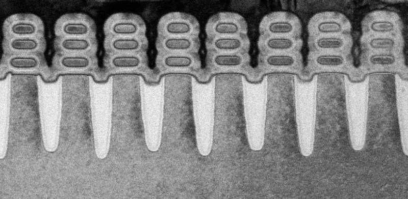
Above: A close-up of IBM’s 5-nanometer transistors. The circuits are 5 billionths of a meter apart.
IBM said the resulting increase in performance will accelerate cognitive computing, the Internet of Things (IoT), and other data-intensive applications delivered in the cloud. The power savings could also mean that the batteries in smartphones and other mobile products could last two to three times longer than today’s devices before needing to be charged.
Scientists working as part of the IBM-led Research Alliance at the SUNY Polytechnic Institute Colleges of Nanoscale Science and Engineering’s NanoTech Complex in Albany, N.Y. achieved the breakthrough by using stacks of silicon nanosheets for the transistor, instead of using the standard FinFET architecture, which is the blueprint for the semiconductor industry up through 7 nanometers.
IBM also said the improvement provides a significant boost in terms of meeting the future demands of artificial intelligence (AI) systems and virtual reality and mobile devices.
Nanosheets represent a new direction, but Khare said IBM Research has been exploring the technology for more than 10 years. This work is the first time that stacked nanosheet devices have shown advantages in electrical properties over the prevailing FinFET architecture. With this technology, Khare believes that the industry can stay on its path of progress every two or three years.

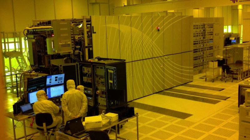
Above: IBM’s 5-nanometer manufacturing equipment.
“The work is to continue to push and innovate so we can be on par or better than Moore’s Law,” said Khare. “This shows with the right investment one could continue to push semiconductor technology. This is how 5 nanometers can be put together.”
The transistors are built with Extreme Ultraviolet (EUV) lithography, which is used to stencil the circuit designs on chips. With EUV lithography, the width of the nanosheets can be adjusted continuously, all within a single manufacturing process or chip design. One of the achievements of the technology is that it can be built using the same manufacturing steps and processes used in 10-nanometer manufacturing.
The flexibility of nanosheets permits the fine-tuning of performance and power for specific circuits — something not possible with today’s FinFET transistor architecture, which is limited by its current-carrying fin height. Therefore, while FinFET chips can scale to 5 nanometers, simply reducing the amount of space between fins does not provide increased current flow for additional performance.
IBM said three years ago that it would invest $3 billion over five years in chip research and development, and this is one of the results of that commitment. IBM Research has more than 3,000 researchers in 12 labs.
Above: IBM’s 5-nanometer production equipment.