IBM Research said recently it could keep Moore’s Law on track with a new 5-nanometer prototype chip. But Globalfoundries has something just as good for the longevity of the chip industry: a new 7-nanometer manufacturing plant.
The semiconductor industry thrives on miniaturization, or making its chips smaller so they can be faster, cheaper, and consume less power. So far this push for progress has upheld Moore’s Law, the notion observed by Intel chairman emeritus Gordon Moore, who said in 1965 that the number of transistors on a chip doubles every year (he later changed it to every couple of years). Ever since, Moore’s Law has driven the industry on a steady drumbeat of innovation.
IBM’s 5-nanometer chip is a big advance compared to today’s 10-nanometer chips (a nanometer is a billionth of a meter). But it will take IBM and its partners a while before they can make millions of such chips in a factory.
However, Globalfoundries said that its 7-nanometer FinFET manufacturing technology will be ready in the first half of 2018. The chips based on that manufacturing process will deliver a 40 percent boost in performance, leading to better mobile processors, cloud servers, and networking infrastructure.
June 5th: The AI Audit in NYC
Join us next week in NYC to engage with top executive leaders, delving into strategies for auditing AI models to ensure fairness, optimal performance, and ethical compliance across diverse organizations. Secure your attendance for this exclusive invite-only event.
Globalfoundries said that design kits are available now, and volume production will happen in the second half of 2018.
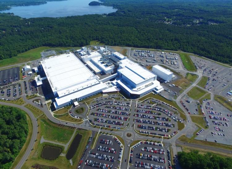
In September 2016, Globalfoundries announced plans to develop its own 7-nm FinFET technology. Thanks to additional improvements at both the transistor and process levels, the 7LP technology is exceeding initial performance targets and is expected to deliver greater than 40 percent more processing power and twice the area scaling than the previous 14-nm FinFET technology. The technology is now ready for customer designs at the company’s Fab 8 facility in Saratoga County, N.Y.
“Our 7nm FinFET technology development is on track and we are seeing strong customer traction, with multiple product tapeouts planned in the next twelve months,” said Gregg Bartlett, senior vice president at Globalfoundries, in a statement. “And, while driving to commercialize 7-nm in 2018, we are actively developing next-generation technologies at 5-nm and beyond to ensure our customers have access to a world-class roadmap at the leading edge.”
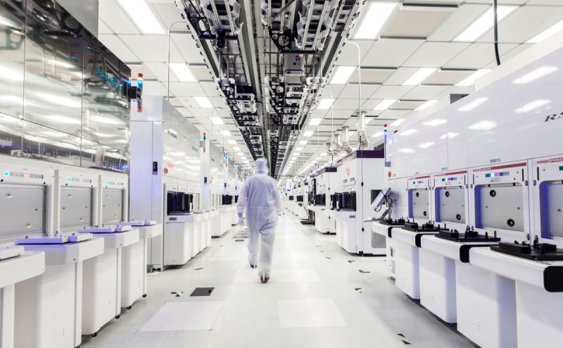
Above: Inside Globalfoundries 7-nm chip factory.
Globalfoundries also continues to invest in research and development for next-generation technology nodes. In collaboration with its partners IBM and Samsung, the company announced a 7-nm test chip in 2015, followed by the recent announcement of the industry’s first demonstration of a functioning 5-nm chip using silicon nanosheet transistors.
“We are very pleased with the leading-edge technology that Globalfoundries is bringing with its advanced 7-nm process technology,” said Mark Papermaster, CTO and senior vice president of technology and engineering at Advanced Micro Devices, in a statement. “Our collaborative work with Globalfoundries is focused on creating high-performance products that will drive more immersive and instinctive computing experiences.”
Dan Hutcheson, chairman of analyst firm VLSI Research, said in a statement, “Globalfoundries continues to demonstrate America’s leadership in advanced technology. If they continue this progress on 7-nm, Globalfoundries will be the first company to leapfrog a full node (from 14-nm to 7-nm, skipping 10-nm). Everyone that’s tried it in the past has failed well before this point in the process. It’s a completely new strategic approach for extracting value from Moore’s Law. By biting the bullet and skipping 10-nm, Globalfoundries opened up the technical bandwidth to attack 7-nm head-on. Others have been dividing their resources and going for half- or even quarter-nodes.”