The future of Intel is AI. Its books imply as much. The Santa Clara company’s AI chip segments notched $1 billion in revenue last year, and Intel expects the market opportunity to grow 30% annually from $2.5 billion in 2017 to $10 billion by 2022. Putting this into perspective, its data-centric revenues now constitute around half of all business across all divisions, up from around a third five years ago.
Still, increased competition from the likes of incumbents Nvidia, Qualcomm, Marvell, and AMD; startups like Hailo Technologies, Graphcore, Wave Computing, Esperanto, and Quadric; and even Amazon threaten to slow Intel’s gains, which is why the company isn’t resting on its laurels. Intel bought field-programmable gate array (FPGA) manufacturer Altera in 2015 and a year later acquired Nervana, filling out its hardware platform offerings and setting the stage for an entirely new generation of AI accelerator chipsets. Last August, Intel snatched up Vertex.ai, a startup developing a platform-agnostic AI model suite.
Intel’s got plenty on the front burner, needless to say — so much that it’s tough to keep track of it all. But vice president and architecture general manager Gadi Singer was happy to provide us guidance in a recent interview. So was Casimir Wierzynski, a senior director in Intel’s artificial intelligence product group, who offered a glimpse into Intel’s work in light-based, AI-accelerating photonic circuits and optical chips.
“AI hardware is a multibillion-dollar opportunity. The fact that we can and we will invest in several product lines is because the needs are going to range [widely] — some are going to be focused on things like acceleration with a lot of power efficiency sensitivity, which are different from others,” Singer said. “So this is an area that is worth investing in a complementary portfolio.”
June 5th: The AI Audit in NYC
Join us next week in NYC to engage with top executive leaders, delving into strategies for auditing AI models to ensure fairness, optimal performance, and ethical compliance across diverse organizations. Secure your attendance for this exclusive invite-only event.
Software
Hardware is nothing if it can’t be easily developed against, Singer rightly pointed out. That’s why Intel has taken care not to neglect the software ecosystem piece of the AI puzzle, he said.
Last April, the company announced it would open-source nGraph, a neural network model compiler that optimizes assembly code across multiple processor architectures. Around the same time, Intel took the wraps off One API, a suite of tools for mapping compute engines to a range of processors, graphics chips, FPGAs, and other accelerators. And in May, the company’s newly formed AI Lab made freely available a cross-platform library for natural language processing — NLP Architect — designed to imbue and benchmark conversational assistants with name entity recognition, intent extraction, and semantic parsing.
Singer noted that these are not the only toolkits Intel has open-sourced. It now offers its neural network distiller library, which can be used to strip away bits of AI models irrelevant to a target task in order to shrink the size of these models. There’s also Coach, a reinforcement learning framework that lets users embed AI agents in training environments targeting robotics and self-driving vehicle scenarios.
Spring 2018 saw the launch of OpenVINO (Open Visual Inference & Neural Network Optimization), a toolset for AI edge computing development that packs pretrained AI models for object detection, facial recognition, and object tracking. It works with traditional CPUs or chips specially made for inferencing (the point in time at which a trained AI model makes predictions) like FPGAs, and it has already been deployed by companies such as GE Healthcare for medical imaging and Dahua for smart city services.
Singer said OpenVINO is intended to complement Intel’s Computer Vision software development kit (SDK), which combines video processing, computer vision, machine learning, and pipeline optimization into a single package, with Movidius Neural Compute SDK, which includes a set of software to compile, profile, and check machine learning models. They’re in the same family as Intel’s Movidius Neural Compute API, which aims to simplify app development in programming languages like C, C++, and Python.
Many of these suites run in Intel’s AI DevCloud, a cloud-hosted AI model training and inferencing platform powered by Xeon Scalable processors. DevCloud offers scalable storage and compute resources and enables developers to remotely test, optimize, and validate models against hardware, such as mini-PCIe development boards from manufacturers like Aaeon Technologies.
Privacy
Intel is cognizant of the trend toward privacy-preserving AI training and inferencing, said Singer, who pointed to the open-sourcing late last year of HE-Transformer as an important first step. At a high level, HE-Transformer is an nGraph backend based on Microsoft Research’s Simple Encrypted Arithmetic Library (SEAL) that allows AI models to operate on encrypted data.
The “HE” in HE-Transformer is short for “homomorphic encryption,” a form of cryptography that enables computation on ciphertexts — plaintext (file contents) encrypted using an algorithm. It generates an encrypted result that, when decrypted, exactly matches the result of operations that would have been performed on unencrypted text.
HE-Transformer effectively adds an abstraction layer that can be applied to neural networks on open source frameworks such as Google’s TensorFlow, Facebook’s PyTorch, and MXNet.
“We believe that both security and privacy are going to play a significant role. It’s actually a fundamental enabler of machine learning at scale,” he said. “Privacy questions become significant if you want to … get information for many patients across many hospitals, for example. When you want to learn about the behaviors and movements of these people, if you’re not able to protect their privacy then you won’t be given access to this data.
When asked whether Intel would pursue the development of a machine learning library like Google’s TensorFlow Privacy, which employs a range of statistical techniques to guarantee privacy in AI model training, Singer said that work is ongoing on related tools. “We’re not talking about it at this stage, because it’s very early for our deep learning capabilities,” he said. “But there’s high interest [and] a lot of investment at this point in time.”
Accelerators and FPGAs
The neural networks at the heart of most AI systems consist of neurons, or mathematical functions loosely modeled after biological neurons. These are connected by “synapses” that transmit signals to other neurons, and they’re arranged in layers. Those signals — the product of data, or inputs, fed into the neural network — travel from layer to layer and slowly “tune” the network by adjusting the synaptic strength (weights) of each connection. Over time, the network extracts features from the data set and identifies cross-sample trends, eventually learning to make predictions.
Neural networks don’t ingest raw images, videos, audio, or text. Rather, samples from training corpora are transformed algebraically into multidimensional arrays like scalars (single numbers), vectors (ordered arrays of scalars), and matrices (scalars arranged into one or more columns and one or more rows). A fourth entity type that encapsulates scalars, vectors, and matrices — tensors — adds in descriptions of valid linear transformations (or relations).
A single image containing millions of pixels, for instance, might be transformed into a large matrix of numbers, while words and phrases from utterances in an audio recording might be mapped to vectors, a technique known as embedding.
Some hardware handles these statistical operations more efficiently than others, unsurprisingly. Processors are generally sufficient for inferencing and some training involving complex sequential calculations — particularly those like Intel’s second-generation Xeon Scalable CPUs, which boast a combination of vector neural network instructions and deep learning software optimizations dubbed DL Boost AI. To that end, Intel claims its second-generation Xeon Scalable CPUs provide up to 2.4 times performance on AI workloads that account for 60% of datacenter inferencing and up to 14 times performance with respect to inferencing workloads, including image recognition, object detection, and image segmentation. The company also claims its forthcoming 10-nanometer Ice Lake architecture will offer up to 8.8 times higher peak AI inferencing throughput than comparable products on the market.
But some of the most demanding deep learning tasks involve tensor operations, and graphics cards and specially designed chips called application-specific integrated circuits (ASICs) are more conducive to these operations. That’s because they contain thousands of cores capable of performing millions of mathematical calculations in parallel.
“Even though for inferenc[ing] the CPU is very effective, there are cases where you need to do tensor operations. The most demanding tasks in deep learning is working with … multidimensional arrays and doing all the arithmetic on tensors.” he said. “[From] a solutions architecture perspective, continuously enhancing CPUs, both in terms of optimizing software and additional hardware features, makes sense … [but] CPUs by themselves aren’t going to be sufficient to cover all these types of [use cases].”
Consider a vision processor like Intel’s 16nm Myriad X VPU. It’s optimized for image signal processing and inferencing on-device, with a stereo block that can process dual 720p feeds at up to 180Hz and a tunable signal processor pipeline with hardware-based encode for up to 4K video resolution across eight sensors. It also has Intel’s Neural Compute Engine, a dedicated hardware accelerator with native FP16 support and fixed-point 8-bit support.
Intel claims the chip can hit 4 teraflops of compute and 1 trillion operations per second of dedicated neural net compute at full blast, or about 10 times the performance of its predecessor (Myriad 2) in deep neural network inferencing.
FPGAs aren’t quite like purpose-built accelerators in that their hardware tends to target general, broader compute and data functions. But they do have an advantage in their programmability, which enables developers to configure and reconfigure them post-manufacture. That’s likely one of the reasons Microsoft chose Intel’s Stratix 10 FPGAs for Project Brainwave, a cloud service optimized to accelerate deep neural network training and deployment.
Intel offers at-the-edge FPGA solutions in Agilex, its new collection of 10nm embedded chipsets designed to address “data-centric” challenges in enterprise networks and datacenters.
Agilex products feature a customizable heterogeneous 3D system-in-package comprising analog, memory, computing, and custom I/O components — including DDR5, HBM, and an Intel Optane DC. They’re fully supported by Intel’s One API and offer a migration path to ASICs.
Intel claims that Agilex FPGAs are capable of 40% higher performance or 40% lower total power compared with Intel’s long-in-the-tooth 14nm Stratix 10 FPGAs, thanks in part to their second-generation HyperFlex architecture.
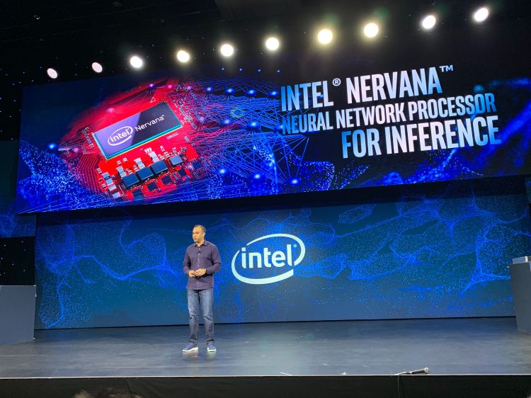
Achieving Nervana
Intel first announced that it was working on two AI accelerator chips — one for inferencing workloads and one for training — back in 2017, and it further detailed the inferencing product in January during a press conference at the Consumer Electronics Show (CES). Called the Nervana Neural Network Processor (NNP-I), it fits into a PCIe slot (or comes in a mezzanine board based on the OCP Accelerator Module specification), is built on a 10nm process, and will include processor cores based on Intel’s Ice Lake architecture to handle general operations, as well as neural network acceleration.
The NNP-L is optimized for image recognition and has an architecture distinct from other chips; it lacks a standard cache hierarchy, and its on-chip memory is managed directly by software. Singer says that because of its high-speed on- and off-chip interconnects, the NNP-L is able to distribute neural network parameters across multiple chips, achieving very high parallelism. Additionally, it uses a new numeric format — BFloat16 — that can boost the sort of scalar computations central to inferencing tasks, enabling the chip to accommodate large machine learning models while maintaining “industry-leading” power efficiency.
“Images are probably the use case that’s most applicable for accelerators, because so much of image recognition [is] matrix multiplication functions,” said Singer. “When you go to natural language processing and recommender systems, there’s a greater blend of types of compute that’s required … [The] CPU cores on-die [let you do a] high mix of heavy tensor activity and do [CPU tasks] locally without having to move the data off-chip.”
Mass production of NNP-I remains a ways off, but Singer says that it’s already running multiple topologies in Intel’s labs. He expects it’ll go into production this year with support for Facebook’s Glow Compiler, a machine learning compiler designed to accelerate the performance of deep learning frameworks.
The aforementioned accelerator chip — Nervana Neural Net L-1000, code-named “Spring Crest” — might arrive alongside the NNP-I. The 16nm chip’s 24 compute clusters will deliver up to 10 times the AI training performance of competing graphics cards and 3-4 times the performance of Lake Crest, Intel’s first NNP chip.
Singer wasn’t willing to reveal much more but said additional details about Spring Crest will be revealed in the coming months.
Seeing the light
What lies beyond the NNP-I and Spring Crest might look very different from the AI accelerator chips of today, according to Wierzynski, who directs Intel’s silicon photonics group under the AI products division. There, work is underway on photonic integrated circuits — the foundations of optical chips — that promise a host of advantages over their electronic counterparts.
“One thing that caught my eye a couple of years ago was a paper that came out of MIT,” Wierzynski told VentureBeat. “It basically asked, ‘Hey, instead of using electronics, why don’t you guys think about using photons?’ Photons have these really nice properties, and they can move really quickly through matter, and there’s ways of controlling light so that it can do useful things for you.”
Wierzynski was referring to a 2017 paper coauthored by Yichen Shen, the CEO of Boston-based photonics startup Lightelligence. Shen, then a PhD student studying photonic materials at MIT under Marin Soljacic, a professor at MIT’s Department of Physics, published research in the journal Nature Photonics describing a novel way to perform neural-network workloads using optical interference.
“One of the key issues around accelerating deep learning is how do you meet this need for lower and lower latency when chips keep shrinking more and more?” said Wierzynski. “We’re really pushing the limits of what silicon can do. One of the ways this shows up is you want a certain amount of compute performance but within some manageable amount of energy consumption.”
To that end, optical chips like Lightelligence’s require only a limited amount of energy, because light produces less heat than electricity. They’re also less susceptible to changes in ambient temperature, electromagnetic fields, and other noise.
Moreover, latency in photonic designs is improved up to 10,000 times compared with their silicon equivalents, at power consumption levels “orders of magnitude” lower. And in preliminary tests, certain matrix-vector multiplications have been measured running 100 times faster compared with state-of-the-art electronic chips.
“The hope is that you would be able to use [AI] models that are fairly close to what people are using now,” said Wierzynski. “[We’re] learning more about how you could build photonic circuits at scale. It sounds like Star Trek.”
It won’t be easy. As Wierzynski noted, neural networks have a second basic building block, in addition to matrix multiplications: nonlinearities. A network without them simply computes a weighted sum of its inputs and can’t make predictions. And, unfortunately, questions remain about what kinds of nonlinear operations can be executed in the optical domain. A possible solution is a hybrid approach that combines silicon and optical circuits on the same die. Parts of the neural network would run optically, and parts of it would run electronically, said Wierzynski.
But that wouldn’t solve optical chips’ scaling problem. Speedy photonic circuits necessarily require speedy memory, and then there’s the matter of packaging every component — including lasers, modulators, and optical combiners — on a roughly 200-millimeter wafer.
“As in any manufacturing process, there are imperfections, which means that there will be small variations within and across chips, and these will affect the accuracy of computations,” said Wierzynski.
He and colleagues are chipping away at solutions, fortunately. In a recent paper, they describe two architectures for building an AI system atop Mach-Zender interferometers (MZIs), a type of photonic circuit that can be configured to perform a 2×2 matrix multiplication between quantities related to the phases of two light beams.
After training the two architectures in simulation on a benchmark deep learning task of handwritten digit recognition (MNIST), the researchers found that GridNet achieved higher accuracy than FFTNet (98% versus 95%), when it came to double-precision floating point accuracy. Importantly, FFTNet demonstrated robustness in that it never fell below 50% accuracy, even with the addition of artificial noise.
Wierzynski says the research lays the groundwork for AI software training techniques that might obviate the need to fine-tune optical chips post-manufacturing, saving time and labor.
“It’s kind of a way of taking very sophisticated manufacturing techniques Intel has painstakingly developed over the last few decades for light circuits and giving it an entirely new purpose,” he added. “It’s early days for this kind of technology — there’s going to be a lot more work required in this field — [but] it’s very exciting to me.”