Intel is unveiling packaging innovations for creating three-dimensional chip packages and other solutions that put together multiple chips.
In advance of the Semicon West conference in San Francisco, Intel shared more details on several of its latest packaging technologies, building on previous news related to its Embedded Multi-Die Interconnect Bridge (EMIB) technologies and Foveros 3D chip packages.
Why it’s important
Chip packaging has always played a critical — if under-recognized — role in the electronics supply chain, Intel said. As the physical interface between the processor and the motherboard, the package provides a landing zone for a chip’s electrical signals and power supply. As the electronics industry transitions to the data-centric era, advanced packaging will play a much larger role than it has in the past.
More than just the final step in the manufacturing process, packaging is becoming a catalyst for product innovation. Advanced packaging techniques allow integration of diverse computing engines across multiple process technologies with performance parameters similar to a single die, but with a platform scope that far exceeds the die-size limit of single-die integration. These technologies will improve product-level performance, power, and area while enabling a complete rethinking of system architecture, Intel said.
June 5th: The AI Audit in NYC
Join us next week in NYC to engage with top executive leaders, delving into strategies for auditing AI models to ensure fairness, optimal performance, and ethical compliance across diverse organizations. Secure your attendance for this exclusive invite-only event.
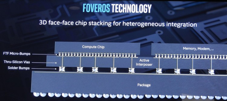
The first disclosure is what Intel is calling co-EMIB. Co-EMIB brings together EMIB and Foveros technologies — already in production today in products such as Intel Stratix 10 field programmable gate arrays (FPGAs), 8th Gen Intel Core processors with Radeon Graphics, and the forthcoming Lakefield 10-nanometer hybrid CPU architecture.

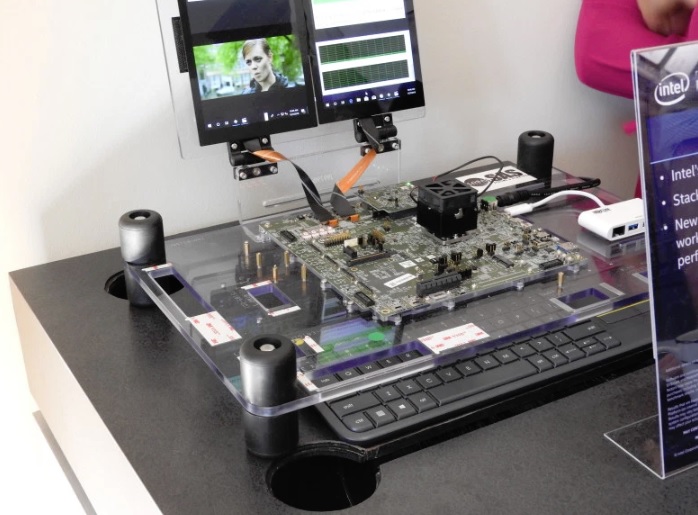
Above: A demo of Intel’s Foveros 3D chip stacking technology last December.
Embedded Multi-die Interconnect Bridge (EMIB) enables the connection of two or more Foveros (3D stacked chip) elements to create a package of chiplets that essentially performs as a single chip. These Foveros elements can also can be connected to analog, memory, and other tiles with very high bandwidth and at very low power. This makes co-EMIB packaging technology ideal for large-die high-performance applications that could otherwise be limited by reticle size.
Intel is also showing a preview of Omni-Directional Interconnect (ODI) technology. ODI, the next step beyond co-EMIB, will bring together the best of EMIB and Foveros, plus additional technology innovation to provide even greater flexibility for communication among the chiplets in a package.
In short, the top chip in a stack can communicate horizontally with other chiplets, similar to EMIB. It can also communicate vertically through TSV connections in the base die below, similar to Foveros. Additionally, ODI leverages large vertical vias to allow power delivery to the top die directly from the package substrate.
Much larger than traditional TSVs, the large vias have lower resistance, which the company says provides more robust power delivery with higher bandwidth and lower latency for high-performance datacenter workloads, such as AI and supercomputing. Intel said it is the first in the industry to develop this packaging technology and to begin preparing to move it into its manufacturing process.
Finally, Intel shared more details on a new die-to-die interface called Management Data Input/Output (MDIO), a PHY-level communication protocol that controls the interface between chiplets. The company says MDIO provides better power efficiency and more than double the pin speed and bandwidth density offered by its current Advanced Interface Bus technology, with availability planned for 2020.
“Our vision is to develop leadership technology to connect chips and chiplets in a package to match the functionality of a monolithic system-on-chip,” said Babak Sabi, Intel corporate vice president for test and assembly tech development, in a statement. “A heterogeneous approach gives our chip architects unprecedented flexibility to mix and match IP blocks and process technologies with various memory and I/O elements in new device form factors. Intel’s vertically integrated structure provides an advantage in the era of heterogeneous integration, giving us an unmatched ability to co-optimize architecture, process and packaging to deliver leadership products.”


