Presented by Intel
For more than 50 years, Moore’s Law has paced the advance of electronics, from semiconductor chips to laptops and cell phones. Now, the golden rule of technology price and performance from Intel co-founder Gordon Moore is evolving once again.
Demanding modern workloads like AI often need specialized, high-powered processors with unique requirements. So Intel and other leading-edge chipmakers are turning to innovative new chip design and packaging techniques – and re-writing the rules of digital innovation for a new era.
 Ramune Nagisetty is Director of Process and Product Integration for Intel Technology Development. She plays a lead role in helping the company create a new industry ecosystem around chiplets and advanced packaging.
In this interview, she explains how the revolutionary new approach benefits AI, Intel, industry partners, startups, and investors while evolving Moore’s Law.
Q: At a high-level, what are the new approaches and commercial breakthroughs here?
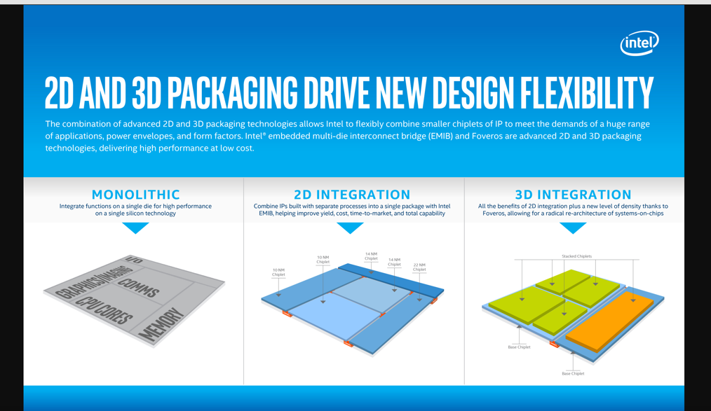
RN: New heterogeneous design and manufacturing techniques break up the key elements of chips – such as compute, memory, modem, graphics – into smaller individual pieces called “chiplets”. With advanced packaging techniques like Intel’s EMIB and Foveros 3D technologies, chiplets can be integrated in both two and three dimensions, horizontally and vertically.
Together, these innovations enable a radically new, mix-and-match approach to chip design. They dramatically increase the range of performance improvement and power savings for a wide array of product applications. They also enable creation of breakthrough architectures and smaller, thinner, lighter form factors and best-in-class products that are not possible with existing approaches. It’s a new kind of catalyst for innovation in the age of Big Data and AI.

Q: So how is this evolving Moore’s Law? What’s the next phase?
RN: Moore’s law is really one of the key drivers for economic productivity and overall innovation. Whether we’re consumers of devices, phones, cloud services, or Gmail, we’re all benefitting from this ongoing improvement in the power and performance benefits of advanced technology. The types of things we enjoy today are a direct benefit from Moore’s law, which is essentially technology scaling.
Moore’s Law was originally about cost per transistor and about how many transistors could be squeezed onto a chip. But it’s evolving. A new, broader view of the power and performance benefits of leading-edge technology is continuing the evolution of Moore’s law. New approaches to architecting computing systems enable the next phase of Moore’s Law by removing traditional bottlenecks and improving performance, power, and cost.
Drivers
Q: Why are chiplets and advanced packaging emerging now?
RN: We’ve actually been working on these technologies for a really long time. I started working on chiplet architectures in 2010; the first paper on Intel’s EMIB (embedded multi-die interconnect bridge) technology was published in 2011. But it’s the use case that ends up driving when technology becomes relevant. The inflection point can be traced back to around 2012, when AlexNet won the ImageNet AI challenge for recognizing and classifying visual objects. That was actually the beginning of neural nets gaining practical applicability. Neural nets often rely on having access to large capacity, high-bandwidth memories, which are typically integrated inside the package. And so that was the toehold for advanced package-level integration.
Today some chips are just too large, and they need to be broken up into smaller pieces because they don’t fit within the lithographic reticle limit. They’re larger than can be printed. But with advanced packaging, smaller chiplets can be stitched back together in innovative new ways.
And in some cases, silicon technology is very specialized for specific types of uses. It may be mostly optimized for digital, for example, and we may want to optimize for analog. And so when we start talking about creating more specialized products, this is where chiplets really come into play.
Q: Why has chip specialization become so important?
RN: We’ve basically been using a general-purpose approach for a really long time. And in any industry, whether you’re talking about silicon or automobiles or boats or airplanes, at some point the general-purpose approach doesn’t yield as great a benefit than if you create highly specialized products for specific applications. And so we have different types of cars and trucks and airplanes for different purposes. We’re in a similar situation with chips.
Look how pervasive computing has gotten. It’s woven through our entire lives, from sensors to cell phones to laptops and gaming platforms to cloud computing. The range of applications is so broad now that you really do have to start specializing. And specializing is where you get a lot of benefit for the different use cases and workloads. How those benefits will continue to be realized in the future will be based on using specialized chiplets for specific use cases such as graphics and AI workloads.
Applications
Q: What are the top use cases for chiplets and advanced chip packaging right now?
RN: Neural nets is one. The pace of change that’s happening with their algorithms makes them a good candidate for this type of integration. Different companies may want customized neural nets as well. You already see companies like Google creating their own chips such as the Google TPU (tensor processing unit) for their own applications. Companies want specialized processors for specific algorithms.
The other natural application is high-speed transceivers. They’re very challenging to design and validate. Companies definitely want to use best-in-class transceivers, but they don’t want to necessarily design them themselves. I was meeting recently with industry leaders at a working group of the Open Compute Project (OCP), of which Facebook is a big sponsor. Leaders from across the industry recognized the challenges in building high-speed transceivers and agreed this would be a natural application for the chiplet approach.
Q: Customized silicon, like Field Programmable Gate Arrays and ASICS, are forecast to grow hugely over the next five years, mostly because of AI. These seem like naturals for chiplets …
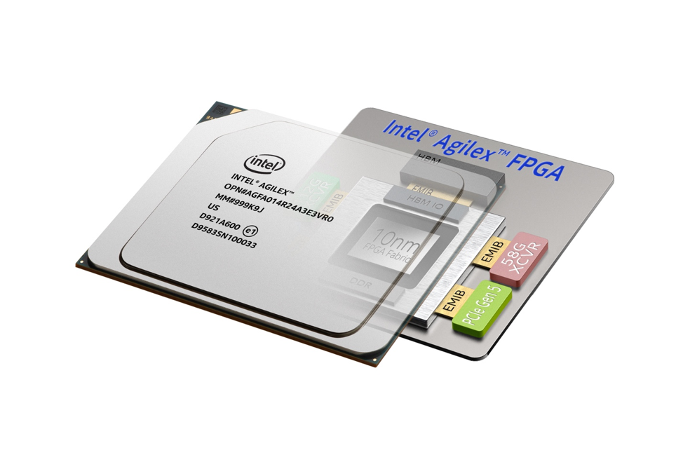
RN: FPGAs really are the epitome of mix and match. In fact, Intel Stratix 10 FPGAs were our first product to use the chiplet and advanced packaging approach. And we are continuing to push the limits of this approach with our next-generation Agilex FPGAs. They’re a great example of a reconfigurable, low-power-consumption chip for AI and analytics at the edge, in the cloud, and on the network.
The ability to customize rapidly is of huge value. Microsoft, for instance, is using high-performance FPGAs in its Project Brainwave platform for continuous rapid innovation and improvement. They’re using FPGAs as a way to learn and develop real-time AI algorithms as quickly as possible, and get those algorithms into deployment.
Using a stepped approach in those kinds of cases is very logical. Once an algorithm has been established as having best-in-class properties – performance or power – you would go from an FPGA, which is a completely flexible piece of hardware, to a structured ASIC, which is an FPGA with a hardened metal interconnect stack. Then you take another step and further harden it into a custom ASIC. We recently acquired a company called eASIC that does just that. It’s a really nice progression and an elegant way to get the best power and performance benefits over time.
Benefits
Q: In what ways does Intel benefit from a mix-and-match approach to making chips?
RN: Combining advanced packaging and the ability to incorporate chiplets that are both internally and externally produced lets us create best-in-class products. Our Intel 8th Gen Core with Radeon RX Vega M graphics product, for instance, had a best-in-class graphics GPU from AMD, and included our own CPU. That’s a somewhat similar strategy for how we created best-in-class transceivers using manufacturing technology external chip foundries.
We also gain a huge improvement in form factor or size. For mobile gaming, for example, fitting inside a laptop design is the crux. So in this case, it’s really optimized for having a best-in-class solution in the smallest size possible.
Q: And OEM’s and other industry partners? How do they benefit?
RN: When I talk to companies that make everything from laptops to server racks, the number one reason they’re going towards chiplets is also to create best-in-class products. It gives them the ability to deliver differentiated products more effectively. It gives them resilience to offer a more reliable cadence of products. And the ability to more nimbly react to new market requirements and to offer customized solutions. Maybe only a certain part of a product needs to be switched-out in order to address a totally new and different market.
So, many of the benefits for Intel are benefits for our OEMs. If we’re able to create best-in-class products more quickly, our partners definitely reap the benefits too.
Q: What about benefits for startups and other innovators?
RN: I think that’s the most exciting aspect of chiplets: opening up platforms for innovation. Over time, due to the massive cost structure in our industry, the increasing costs of designing and manufacturing products have been prohibitive. The chiplet approach can enable smaller, fabless innovators. Some of that is happening through the DARPA CHIPS program, where we have several universities designing chiplets to go into our FPGA platform, and also several startups as well. They don’t need to create the entire CPU, or an entire product, but they can innovate around the pieces that they have expertise in.
Ayar Labs, for instance, has partnered with Intel to create an optical I/O chiplet for high bandwidth, power-efficient communications. That’s just one company that’s been empowered.
So a really critical piece of this is to unlock and unleash the innovation in the ecosystem that I think has become a bit stifled in the old model. It’s exciting.
Q: And for investors?
RN: Much of our economic gains and efficiency over time have been based on the evolution of Moore’s Law, at least for the last 40 years or so. Not just in the semiconductor industry, but in general for economic productivity. I think investors can count on this efficiency continuing to grow because of the ability to create specialized products for specific use cases and workloads.
Recently investing has really been focused on software innovation because of its low barrier to entry. Now, it’s an exciting time for hardware as well, because we can lower that barrier for innovation. And certainly, it’s a great thing for our industry to be able to capitalize on innovation.
Sponsored articles are content produced by a company that is either paying for the post or has a business relationship with VentureBeat, and they’re always clearly marked. Content produced by our editorial team is never influenced by advertisers or sponsors in any way. For more information, contact sales@venturebeat.com.


