
Ever heard of the Hall voltage? Discovered by Edward Hall in 1879, it’s the voltage perpendicular to the flow of a conductor’s charge that’s used to measure the deflection of movement caused by a magnetic field. Critically, it communicates information about the charge carriers in a semiconductor, including the presence of negative electrons and positive quasi-particles (called “holes”) and those particles’ speed in an electric field (as well as their density).
Over a century after the Hall effect was discovered, researchers from KAIST (Korea Advanced Institute of Science and Technology), KRICT (Korea Research Institute of Chemical Technology), Duke University, and IBM claim to have discovered a technique enabling the extraction of even more information from carriers. A paper published this week in the journal Nature describes how the technique could be used to extract carrier lifetimes, diffusion lengths, and metrics regarding recombination (the process by which electrons and holes annihilate each other).
Several studies following the Hall effect’s discovery sought to examine the extent to which the measurement could be performed with photons. In these early photo-Hall experiments, light illumination was used to generate multiple carriers or electron-hole pairs in semiconductors. But because the basic Hall effect provides insights only into the dominant charge carrier (or majority carrier), no attempt was successful in revealing the properties of both carriers (the majority and minority carrier) simultaneously.
June 5th: The AI Audit in NYC
Join us next week in NYC to engage with top executive leaders, delving into strategies for auditing AI models to ensure fairness, optimal performance, and ethical compliance across diverse organizations. Secure your attendance for this exclusive invite-only event.
By contrast, this latest approach — dubbed Carrier-Resolved Photo Hall (CRPH) measurement — starts with a known majority carrier density from the traditional Hall measurement in the dark. Light with a known illumination intensity is then introduced, enabling the discovery of the carrier lifetime and both the majority and minority carrier mobility and density.
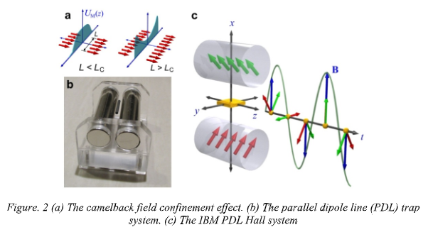
New measuring devices make it easier to orchestrate than before — namely, a tool called the parallel dipole line (PDL) trap. IBM scientists developed the PDL four years ago while investigating the camelback effect, which occurs between two lines of transverse dipoles (pairs of equal and oppositely charged or magnetized poles) when they exceed a critical length. But these researchers later discovered that when rotated the PDL serves as an ideal system for photo-Hall experiments, partly because of the ample space it provides for large area illumination onto samples.
As it turns out, clean Hall signal measurements can be challenging to execute when the signal is weak or unwanted noise is present, such as under lights. They’re best performed with systems like the PDL, which provides an oscillating magnetic field. CRPH helpfully selects both the desired frequency of the target signal and the phase of the field with a method called lock-in detection.
The researchers say their photo-Hall approach allows for the repeatable recording of up to seven parameters from semiconductor measurements, as opposed to the standard three in classical experiments. Furthermore, they say their discovery and technology could help push semiconductor advances in both existing and emerging technologies.
“We now have the knowledge and tools needed to extract the physical characteristics of semiconductor materials in great detail,” wrote contributing authors Oki Gunwan and Doug Bishop in a post published on the IBM Research blog. “For example, this will help accelerate development of next-generation semiconductor technology, such as better solar cells, better optoelectronics devices, and new materials and devices for artificial intelligence technology.”
